Lock Loss
The loss of PLL lock would occur around 980MHz but is wasn't reliable. Sometimes the output would be stable up to 1GHz but then after the unit warmed up a bit it would revert back to the usual behaviour.
This is what the output look like on the spectrum analyzer when the PLL is locked and the frequency relatively is stable (in fact this snapshot isn't all that great - it got better later).

Then if you shift the frequency ever so slightly the output would loose it all together.

The Synchronizer PLLs
The synchronizer has two PLL loops used to lock the output frequency to the 10MHz reference.
In the block diagram below the 'fast' PLL is shown in green and the 'slow' PLL is red. The slow PLL locks a 87-122MHz VCO to the 10MHz reference. The fast PLL divides down the output using a set of frequency dividers

The way it all works is that there are a few paths depending on the frequency range.
- Below 20MHz the output is generated by mixing the VCO output with the 100MHz reference signal generator off the converter board. In this case the output is not fed back through the PLLs.
- Above 20MHz but below 70MHz the output frequency is band-pass filtered and fed to the PLLs
- Above 70Mhz and below 700MHz the output signal is divided by 10 and then fed to the fast PLL and the 700Mhz fed to the fast PLL
- Above 700MHz the output is mixed with a 1200MHz signal derived from the 600MHz IF generated on the IF board to down covert the frequency to 0..700Mhz. This is then divided by 10 to get 0..70MHz which is fed to the fast PLLs. The 700Mhz is again fed to the slow PLL
- Above 1200MHz the output is mixed with an 1800MHz signal generated from the 600MHz IF and the 0..700Mhz fed to the PLLs as above.
When the output is below 20MHz the slow PLL locks the VCO to the 10MHz signal. There is a phase comparator that compares the VCO output with a 10kHz and a 1kHz signal generated from the 10MHz reference. Because the 100MHz this is later mixed with is also locked to the 10MHz reference then this is all that is required.
When the output is above 20MHz the slow PLL takes the 0..70MHz signal derived from one of the paths listed above is divided by a factor K and compared with the 1kHz and 10kHz reference derived signals and used to control the VCO. The VCO is then divided by 64 to generate a signal between 1.5Mhz and 1.9Mhz that is fed to another phase comparator and then used to control the output frequency.
The fast PLL does its own division of the 0..70Mhz signal (divides by M and then by N) to generate a frequency around 1.5MHz to 1.9MHz which gets fed to the phase comparator described above. The fast PLL has extra logic for sweeping so it can lock just at the beginning of a sweep and can handle fast frequency transitions that the slow PLL can't.
Debugging PLLs
So I was dreading this problem because of the PLL loops. The problem is that if the loop is out of lock then all of the loop is out of lock and it's hard to tell where in the loop the fault lies. In this case it is even worse because there are two PLL loops.
Initially I mistakenly thought I could check the slow PLL on its own. I thought it was totally derived from the reference and so should remain in lock regardless. That isn't the case as it does depend on the output. Therefore if the output is unlocked so is the slow PLL and the VCO.
With a brief warm up I could get the unit so it would be in lock and then if I shifted the frequency just a bit it would lose lock. This made debugging easier as I could compare the 'working' with the 'unlocked' states quite easily.
So I started with the slow PLL and began with the VCO. I found that when the loop is locked the VCO frequency was stable but when it lost lock the frequency would jitter. Also I found that the frequency would go to 132MHz which is outside the specified range. Stepping back through the VCO inputs I found that the control voltage was hitting the limits (going to zero) when it lost lock. I walked back further and found the two phase comparison signals (PHKOM11 and PHKOM12) coming from the digital board were hitting the rail (15V) when the PLL lost lock.
Digital Section
Debugging the digital section wasn't much fun. It has two SMB connectors through to the motherboard and I didn't have any SMB patch leads - I have SMC and SMA (both of which are used in this instrument) but not SMB. This meant I can't run the board on risers as the signals on the coaxial connectors are required to debug the PLL loop. I found I could connect to the test points with a wire and then stuff the board back in the unit.
First I looked at the test-points around the dividers (see below). To be honest I don't really understand this circuit. It's a messy mix of ECL and TTL with lots of TTL to ECL conversion going on. There are ECL D type flip-flops feeding ECL counters that adjust to either count by 10 or 11(??).

The core of this is this two chip set that implements a pre-scale and phase comparator. This is the HEF4751VD and HEF4750VD. The pre-scaler has more capability than what is used here but the circuit seems to be controlling these two 4 bit registers that are used to subtract from the count (to adjust the divide ratio). There is a feedback path that clocks out signals that then adjust the counters feeding into the pre-scaler.
Ok so I got a bit lost here but I could see the 10kHz and 1kHz signals at P9 and P10. When the loop lost lock the frequency of these would drop just a little. The phase comparator output would alter also and that matched what I was seeing on the analog board.
So the question is why is this happening? I thought about maybe the counters are not being setup correctly so the division ration is wrong, I traced signals in to check that they aren't being lost (and they weren't). It seemed to be working apart from the fact that it lost lock.
It was about here that I realized that the input is a 700Mhz signal and not the VCO. I also realized that if either PLL was wrong they would both lose lock.
I start looking at the fast PLL - I looked at the frequency of the P11 signal. This signal has already been divided by 10 on the analog board and is divided by another 1,2 or 4 depending on how many of the D flip-flops are enabled by the multiplexer (D140).
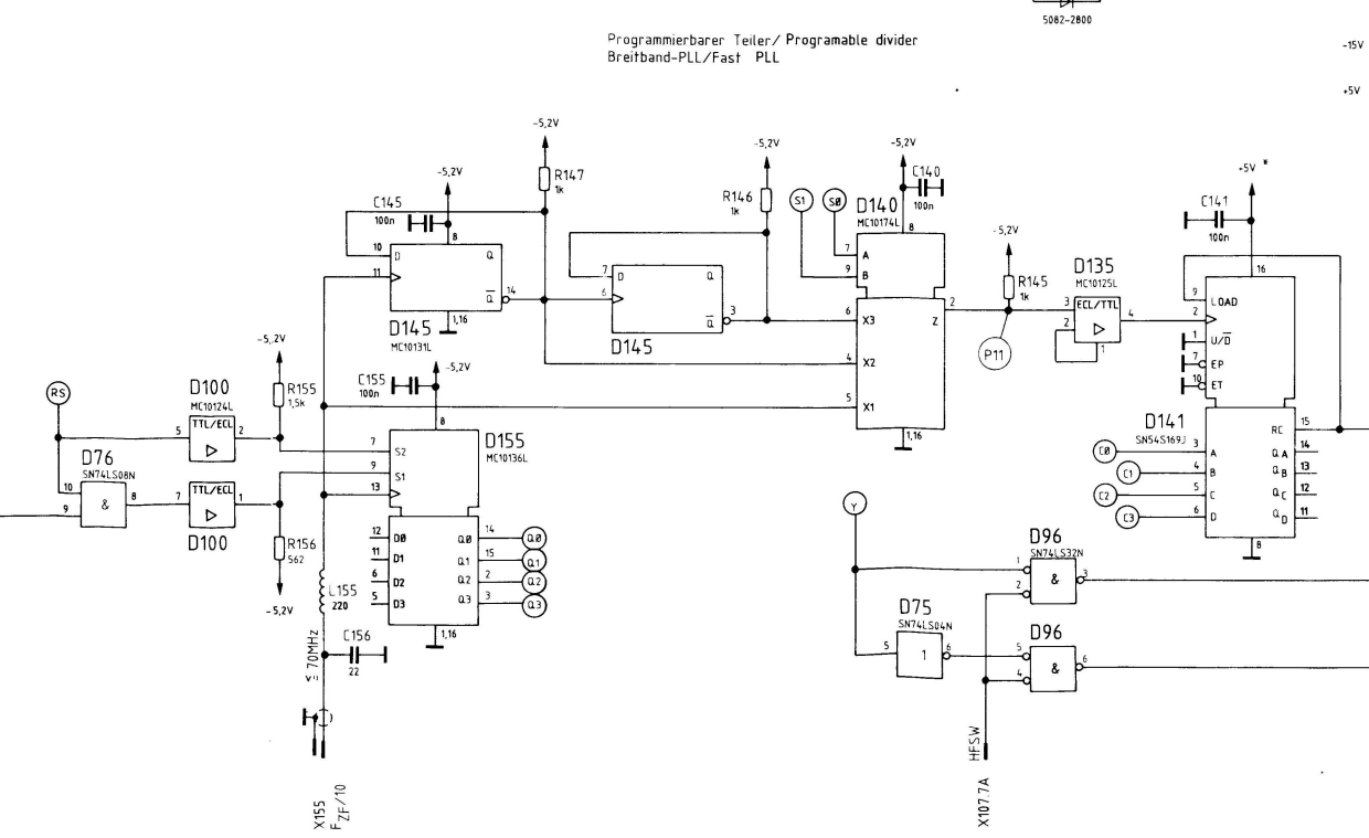
You can figure out the division easily from the table provided in the service manual below. You take the output frequency, work out the down converted freqency by subtracting it from either 1200 or 1800 (or don't subtract if it is less than 700Mhz) and you look up this frequency in table. Then you divide the frequency by M and that should be the frequency at P11.

Again I found this matched exactly - or at least it did when the PLL was locked. When it fell out of lock the frequency would wander off (lower).
New Piece of Test Gear
Up to this point my only way of checking the output frequency above 300MHz was with my spectrum analyzer and I wasn't confident this was correct. A while ago I ordered a pre-scaler for my frequency counter from this polish eBay seller and it finally turned up. The quality of the board and the wiring etc was excellent. I installed this in my 53131A and did some tests. It happily counts -30dBm signals up at 2.5GHz.
Tuning the YIG
One thought I had was that because the YIG output was very out of tune that this could effect the synchronizer PLL's ability to lock. Up to this point I could adjust it as I couldn't measure the output with any accuracy. I followed the procedure to adjust the low end (10MHz) and then the high end (2.5GHz) using my new pre-scaler.
Then I tried the synchronizer again - and it locked at 2.5GHz!
The problem was simply the YIG being too far out.
That was too easy. Well at least I learned a few things.
Final Cleanup
So here it is in my bench (gee it's getting crowded!).

I even took the time to polish up the BNCs with a bit of aluminium polish and a Dremel tool. They look good!


