Friday, 10 April 2015

Lab Power Supply Project - Voltage Regulator

I thought to begin with I would design the voltage regulator part of the lab supply. I can get this working independently of everything else pretty much. The regulator will set the output voltage between 0-30V (from a 30V, 160VA transformer) at 3A or 0-15 at 5A.

Bulk Capacitor

The bulk charge storage capacitors(s) determine the ripple and therefore the maximum output voltage. The ripple voltage is determined by the size of the capacitor and the current we are pulling out of the supply. Wikipedia pretty much explains it here.

The worst case is where the supply is running in the 15V mode at 5A. To limit the ripple to around 5V we require 10,000uF (10mF) of capacitance.

The issues with selecting the capacitors are:
  • The more capacitance the greater the in-rush current when the supply is turned on
  • Less capacitance means greater ripple, lower output voltage and more dissipation in the pass transistor.
  • Cost. More below.
The bulk capacitor has to be rated for 63V and has to be rated for 105 degrees C operation for longevity. When you add all this up it means expensive capacitors. I found some RS branded 4700uF ones for around $5 each but name brand ones can be as much as $10 each.

Voltage Doubler

As mentioned previously, the plan is to use an N-channel MOSFET as the pass element but this means the gate voltage needs to go up well above the output of the power supply (5-10V). To achieve this I have to either lower the maximal output voltage or find a way to generate this voltage.  The problem with lowering the output apart from wasting the capabilities of the transformer is that it will generate a lot more heat in the MOSFET. So the plan is to use a voltage doubler to generate the gate bias.

The image above shows the basics of the voltage doubler circuit. The AC voltage source models the voltage coming from the transformer and the 1k resistor on the right models the load generated by the gate drive circuit.

The two diodes D1 and D2 together with the two capacitors C1 and C2 form the voltage doubler. The diodes charge the capacitors to the AC peek voltage above or below the other AC rail. The effect is that the total charge across both capacitors is double the input voltage.

With load this will fluctuate greatly so I added D4 and the C4 to smooth the output. Here is the simulated output


You can see we now have around 80V with a few volts of ripple. The gate drive only really needs to be a few volts above the desired output and that will be covered below.

The problem with this circuit is that it doesn't behave well when AC1 and AC2 are connected to a bridge rectifier supplying the main part of the PSU. There is a much simpler circuit that only requires two diodes and two capacitors but initially I had problems simulating this in LTSpice. After some Googling I discovered what I needed to do was to attach a 1M resistor between AC2 and ground as otherwise it things this net is floating. See below - the gate drive is being fed to the 10K resistor (the resistor is acting as a load).


This works as before although it has a little less capacitance so can't supply as much current.


Now we need to keep the gate bias below around 44V (see below) so the easiest thing to do here is to use a transistor with a zener diode as a rudimentary regulator. I can't use a real regulator (like say a LM317) as I can't find one that can go up to 40V. I might change this later but as I don't need any sort of precision here it doesn't matter. Here is the gate bias circuit with regulation:


For some reason. even though the zener's breakdown is listed as 40V it drops around 44V. This is near enough for now.

Regulator

In its most basic form, the regulator is actually quite similar to the dummy load I built before. An op amp compares the voltage at the source of a MOSFET with a set voltage and adjusts the gate voltage so that the source matches the set voltage.

The first problem is that the voltages are quite high. The gate voltage (depending on the MOSFET) could need to be as high as 10V above the source which means 10V above the output or 40V. Lots of op amps can't handle 40V supply rails. I found a couple that can and the first one I tried was a LT6016. Here is the basic circuit with a not-so-carefully chosen MOSFET and some loop compensation. The output of the transformer is 44V which is 30V * SQRT(2). The output is set to 30V and there is a pulsing current load of 5A on the output.


While the output voltage does remain a constant 30V, this circuit has a bunch of limitations. The regulator is really slow - it takes a long time to react to changes in input and in particular to changes where the load drops.

The obvious thing to do is to add some output capacitance to keep the output voltage constant. The one issue with this is that it also tends to hold the output up when the load drops so it also makes sense to add a small bit of permanent load to the output.

This didn't really speed up the response that much even though it did reduce the size of the voltage spike. I then thought that perhaps the problem could be with the current drive to the MOSFET gate. I experimented with push-pull drives but eventually found that a simple emitter follower improved the performance considerably!

Tim on EEVBlog suggested I use a pole-zero compensation on the op-amp. Essentially I added a resistor with the capacitor.

Better Simulation

I want to make sure the regulator is going to be stable pretty much regardless of what you connect to the output of the supply. Importantly, the regulator has to be stable if the load is inductive or capacitive.

Tim on EEVBlog pointed out that modeling the load as a current source is not very useful and it would be better to model as a switch with resistor. In the circuit below I have added a small inductance in series with two resistors and a switch. The switch is controller by a voltage source which opens and closes the switch every 10ms. The resistances are chosen to draw 3A at 30V output and drop back to 1.5A (this is in line with the Agilent PSU specification where they claim the supply recovers to within 15mV of the set voltage within 60us when the load switches from half to full current or vice versa).


I experimented with more or less inductance but found that adding more actually made the response better as it reduce the voltage spikes.

I also discovered a better way to model the input voltage so it includes the inductance of the transformer windings. The way this works is you create two coils and use the K spice directive to specify the coupling between the coils. The voltage ratio is determined by the square of the inductance ratios. See here for a better explanation. 

While experimenting with the closed loop frequency response of the regulator, I realized that the output capacitor has a big effect. In particular the output capacitors ESR will effect the pole created by the capacitor. To model this I added a small series resistance with the output capacitor and chose the resistance from datasheets for similar capacitors on RS.

I experimented with adding large capacitance to the output and in the extreme cases this could make the loop unstable.

Voltage Sense

When the supply is pushing 5A even quite thick wires are likely to have significant losses (a few mV at least). To combat this my plan is to implement a voltage sense system to read the voltage off the front terminals. The circuit as it is currently drawn can sense the positive voltage at the output but if there is resistance in the negative path the output voltage won't take that into account.

To get around this I plan to use an op amp to measure the voltage difference and then use this to drive the regulator control loop. The amplifier has the same compensation that was added to the main voltage regulator error amplifier.


Protection

Other protections I added were:
  • A diode to bypass the MOSFET if the output voltage is higher than the voltage on the bulk capacitor.
  • A zener diode between the source and gate terminals of the MOSFET to ensure that the gate never goes above the MOSFET's Vgs limit.
I was also experimenting with over voltage protection. One issue with adding a larger output capacitor or connecting a heavily capacitive load to the supply is that the MOSFET can't lower the voltage when the load varies. Having a 'down programmer' (as Agilent call it) or otherwise a MOSFET that can short the output when the voltage goes above the limit can help here. The idea is this will blow the fuse in the event of a large battery being connected or the output being connected to mains ground etc.

I had some problems when the output is heavily capacitive although when I added a realistic ESR for the capacitor I found the supply behaved well. I have to think about that a bit.

Circuit So Far

The regulator circuit is still very much a work in progress. My plan (now that I got some parts) is to build some of this and see how it behaves. There may be other problems the simulation doesn't reveal so I think there is no point getting too far until I try building it.


Monday, 30 March 2015

Lab Power Supply Project

Often I've ended up doing odd things because I only have a single lab power supply. For example when I was experimenting with op amps I first had to figure out how to create a differential supply from a single supply before I could actually do anything. Also when working on the current load I was using the load to sink current from the lab supply so I ended up running my circuit off a 9V battery until I got a better supply worked out.

The other issue is that the supply I have now is quite primitive. It has a fine/coarse voltage adjustment knobs instead of a multi-turn knob, it does display the output voltage and current digitally but the voltage reading is 200mV off. It has a current limit but you can't see what it is set to unless you short the output. The power output is quite good though (0-14V @ 3.2A and 14-29 @ 2.7A). The load regulation is pretty woeful - I'll get to that later. Occasionally it does some odd things in current limiting mode.

The PSU I have is one of these Jaycar ones that Dave Jones reviewed. It's not too bad really overall and it wasn't expensive. We've used it for all sorts of stuff including as PSU for my son's LIPO charger.

The thing that makes this easier is that all of the work I did with MOSFETs, DACs, voltage references etc for the dummy load is directly applicable here. I'm not starting from complete scratch.

The plan

What I would really like is one of these Rigol DP832A. Of course I could buy one but given I an am using this supply to learn about electronics it seemed a perfect opportunity to build one! Not to mention that the DP832A is close to $1000 here in Australia - that gives me a fair budget for the build!

So In general what I'd like is to have two or three output channels and the ability to run two in dual tracking mode. I'd like it to be at least as good as the Jaycar model but more accurate, more programmable and to have a better UI. So I was thinking it would have

  • Two or ideally three output channels (as I said). Probably 0-30V and at least 0-3A. If possible higher current at lower voltages.
  • Current limiting.
  • Digitally settable output voltage - ideally both via keyboard and rotary knob.
  • Display current and power output.
  • Ability to individually turn each channel on or off (ideally with a momentary switch on the front panel)
  • Pretty high precision - 1mV/1mA resolution, fast response, minimal overshoots, very low noise.
  • Over voltage protection, reverse polarity protection (say if you connect a battery) fuses (both mains and DC). Safe grounded chassis, ground terminal on front.
What would be really nice is to:
  • To be able to graph the current/power output like the Keysight bench meters do. Even show cumulative amount of energy consumed by the driven circuit.
  • To have an Ethernet interface. Maybe a web interface or for it to be LXI compatible or both.
  • Some output programmability (LXI). Doesn't have to be quick.
  • Be able to save/load output configuration settings.
  • Maybe experiment with a 3D printed front panel (for buttons and knobs etc)

Architecture


Looking at teardowns and repairs of other lab supplies such as the Rigol and Agilent units,  the usual thing to do is to use a big, custom wound transformer to generate all of the voltages required. These days the only transformers economically available are (a) Torroidal (which is good) and (b) usually have one or two output windings.

The limited taps means either I use one winding per channel or I use multiple transformers. Using one winding per channel doesn't give me any options for saving energy at lower voltage outputs and no options to boost the current at lower voltages.

Also transformers larger than 200VA are quite expensive.

Another factor driving the overall design is that PCB fab houses are much cheaper for smaller boards. A smaller board is easier to debug too.

These facts led me to decide that what I want is three independent channels that have their own circuitry, control and transformer. This way I can get the design of one right and build another two.

My plan is to use a Raspberry PI as the front-panel controller and have it control each channel via an isolated I2C interface. This way the power for the Raspberry Pi and each channel is all isolated (and floating) from every other channel. The Raspberry Pi supports Ethernet, USB, I2C and there are many touch sensitive LCD panels available. The only downside is the Raspberry PI will require a permanently active power supply and a soft button to allow it to shutdown properly. Also the Pi's boot time is quite long but this could be adjusted with some software pruning.

Each channel will include an AVR (Arduino) processor, DACs ADCs, voltage references as well as a thermal management system. Each channel implements its own current limiting, voltage control, current measurement etc and is controller via I2C. Two channels will include extra hardware to allow them to be shorted together (to create a higher voltage output or dual tracking output). Each channel will store calibration data in EEPROM and provide code to calibrate itself via the control interface.

To limit dissipated heat, my plan is to have relays to switch between either both windings in series or both in parallel. I also plan to build a simple pre-regulator circuit but I don't want to use a switching pre-regulator as they generate too much noise.

I plan to use MOSFET devices as the pass element but this might change if I have trouble stabilising the circuit.

The case is still a problem. To achieve 3A @ 30V I need 160VA transformers which are roughly 200mm x 50mm. Three of these with 100mm x 100mm control boards means I need a big box. Large project boxes are quite expensive and (for safety) the box needs to be metal so it can be earthed.

One option is to use an old shuttle PC case.and build a custom front panel. They have good thermal properties but they are still pretty big.

Open Source Tools

After spending all that time fixing my old Tektronix 475 scope it occurred to me that closed source lab/bench tools are a very bad idea. Without the extensive service manual of the 475 the unit would have been in a land-fill right now.

Furthermore, if you want to do something outside the box with a bit of lab gear, if the device is open you should be able to hack it to do what you want.

I doubt this project will ever be seen outside my bench (and this blog) but just maybe one day someone might release a line of open source lab tools that rival the gear from Keysight or Tektronix. 

Devices with lasered off component markings are very much the opposite of what I would want on my bench.

Next

Over the next while I will be working on the voltage regulator circuit, the pre-regulator and then current limiter. I plan to simulate and bread-board or proto-type each stage separately as I go and integrate as much as I can along the way. I do plan to get PCBs made for this eventually.

Welcome to the next six months of my evenings!

So watch this space! More later.

Saturday, 21 March 2015

Dummy Load

I actually finished the dummy load a while ago but have been a bit lax in writing it all up. I wrote about the design including compensating the control loop (to stop it oscillating) in a previous post here.

To complete my dummy load I did a few things:


  1. Found a suitable heat-sink
  2. Ordered a low tempco, 20W 1Ohm resistor
  3. Switched to a precision op amp
  4. Added a LCD screen and an AVR micro-controller. 
  5. I added a voltage reference and used a DAC to drive the opamp.

Heatsink

I ended up going with the flanged version of this heat sink from Jaycar. It's a bit of a beast and appears to be a half-kilo lump of cast aluminium. It claims to have only a 0.78 degree C per watt temperature increase which seems pretty good. The MOSFET I used has a 1 degree per watt temp rise between the case and the die and is capable of withstanding 175 degrees. So the maximum power dissipation if the ambient temperature is say 35 degrees is (175-35)/1.78 = 78W. So at 25V that is over 3A or at 20V it is just under 4A. Pretty good! 

Power Resistor

I ended up buying one of these Bourns 100ppm 1 Ohm resistors. The thing is capable of 20W which means over 4A of load. Under test I found this thing pretty steady. I had trouble at first as I mounted it on an insulating pad and didn't bolt it down tight enough. Once I realized it's metal tag is well insulated (electrically) I mounted it with heat grease tightly onto the heat sink and it performed well outside its specs.

Precision Op amp

I bought one of these LT1006 op amps that have a really low offset voltage, low drift and low noise. Also you can zero out the input offset but in the end I didn't need to do this as it was so small it didn't matter.

Voltage Reference and DAC

I bought a 4.096 voltage reference (LM4040C41IDBZR). This thing is pretty amazing in that it has a 100ppm tempco and even though it is only accurate to 0.5% was dead on 4.096 (according to my multimeters - one of which is in calibration).

I bought a 12 bit DAC (MCP4921) to go with this. This isn't a great unit but I figured it would do. It boasts an integral non-linearity of 0.5 LSBs but when I tested this in the complete system I found it to be a bit worse. To begin with I thought this was the resistor or the wiring losses but I can't see how this would add a non-linear response. See below for details on how I got around this.

I found an Arduino library to make driving the DAC easy here. The DAC interfaces via SPI which makes life pretty easy.

Initially I was aiming for 10mA resolution but when I found the reference was so stable and accurate I thought I'd go for 1mA. Because of the error in the DAC I didn't quite make it but it's pretty close (less than a 1mA off across the full range).

I ended up using a surface mount adapter board to rig these into the final circuit as both parts were only available in this form.

The Brains

So then my plan was to be able to control the thing from a uController. I found one of these cheap encoders and a simple circuit to read them. There is an Arduino library for reading encoders here that works with this. The circuit for reading these is pretty straight forward - the main objective of the circuit is to debounce the switching of the encoder to avoid jumps. The circuit is on the Arduino site here.

I already had one of these Hitachi compatible LCD screens and again there is an Arduino library for writing to them. I hooked this up as per the instructions here and used the Arduino library to write to it.

I added two buttons so I could have one to change the mode and one to enable/disable the output.

Construction

The whole dummy load was built on a piece of matrix board. The matrix board was screwed to the heatsink. Initially I planned to run the load off a 9V battery but I found the LCD backlighting would drain the battery in a very short time. I changed the circuit to have a power socket for an old plug-pack from a junk box and added a 7812 and 7805 regulator to provide power to the circuit.

The back-lighting is still not right. Initially it was quite bright but it made the regulators far too hot. I reduced the intensity but now it is too dim. I might have to re-visit this.


The dummy load sinks current from the red/black terminals on the right hand side. You can see the DAC and the reference on their adapter boards. The tactile switches and rotary encoder are to the right of the LCD screen.

I added a ICSP header next to the Atmega so I could upload the firmware onto the micro controller.

Software

I had been writing bits of code to drive the DAC, read encoders and drive the display but now it was time to put it together. The functions I wanted were:
  1. To be able to set the current down to the milliamp.
  2. Constant current mode where the load extracts a controlled current.
  3. Pulse mode where the load oscillates from zero to the configured current. I wasn't sure what speed would be most useful so decided to support 50Hz, 100Hz and 1kHz
  4. Ramp mode. Note sure how useful this is but after some testing I decided to support only 50 Hz and 100Hz operation for this mode. More on this later.
  5. Single button output activation/disablement.
  6. Shaft encoder to select from ranges of values. Button to switch between the settings being modified.
After developing GUIs for thick client apps as my day-job I found two lines of 16 characters quite limiting. I decided that I wanted four basic fields on the display to be:
  1. The output mode (constant current, pulse, sawtooth)
  2. The mode qualifier (none for constant current mode) which is the frequency of the output for whatever mode is selected
  3. An indicator showing if the output is enabled or not.
  4. The output current.


I wanted to make the field you are currently editing to blink. I couldn't figure out how to make the LCD blink some text. It is likely the LCD can do it but I don't think it can be done if you access  LCD using only a 4 bit wide interface. After some head scratching I figured out I could just get the micro controller to do the blinking by re-displaying the LCD contents with the field blank.

So the basic interface is you hit the mode button (top right) and you can move between fields. The field being edited blinks to show that it is being edited and if you turn the encoder the field cycles through the possible values. At any time if you hit the bottom button (enable/disable) it turns on the output and blinks the 'Enabled' field. When the output is enabled you can't edit anything but you can hit the enable/disable button again to disable the output.

Also the code saves whatever the settings are in NVRAM so if you power cycle the device it comes back up in the mode where you left it (but with the output disabled).

Initially I split the current field into amps and mili-amps (so you could edit the whole number of amps with the encoder, hit mode and then edit the number of mili-amps) but I found that cycling through 999 values in the mili-amps field was too slow. Instead it now is split into amps, 0.1 amps and then mili-amps.

Software Design

At this point I realized this is no longer a trivial application. Ok it isn't that complicated but it isn't ten minutes of coding either.

Working in the Arduino dev studio, I started create classes to model the components;
  1. LoadControl models the DAC and analog electronics and implements setting the output current and output mode etc.
  2. Display manages the display of the LCD fields including blinking fields.
  3. Controller sits between the display, the input devices and the LoadControl and manages the device based on the user's inputs.
Then I needed a few more things:
  1. ButtonMonitor automates interfacing with buttons and provides a function to tell you if the button was clicked. There is one button monitor for each button.
  2. PersistentSettings saves the current user selection in the NVRAM and is used to load the last used settings at startup
  3. Splitting up, updating and re-combining the output current from fields became a bit of a mess so I moved this out into an AmpsSplitter class that handled it all.
The main module simply calls the Controller::update() method in the loop method. The controller:
  • Checks if a the enabled button was pressed and if so switches between enabled/disabled mode.
  • If enabled. checks if the mode button was clicked and if so cycles to the next field
  • Otherwise the code checks if the shaft encoder was changed and if so it cycles the current field by the number of clicks the shaft encoder was turned.
  • Updates the display. This is where the display writes the fields into the LCD. The display also knows which field is blinking and will check the time (using getMilis()) so it can blink the current field every 200ms

Timing


Initially I had the code also calling LoadControl::update() every time round so that if the output is enabled it will update the DAC. The problem is the timing was all over the place and generated unusable amounts of jitter.

The processor has timers you can use to generate interrupts so the processor can act at specific times. There are two timers but I quickly figured out the first timer is used by the getMilis() system call and was too low-resolution for what I wanted.

Using AVR manual and this guide I  set about updating the LoadControl code so that when the output is enabled and not in constant current mode it will use a timer interrupt to time updates to the DAC. This worked very well and could handle updates as fast as 10kHz. Much faster than this it would slow the user interface down so much that it became unusable.

The basic idea is there is a register that counts each CPU clock cycle. You can set a value so that when the counter equals the value an interrupt is generated. The counter is only 16 bit however and the clock speed is 16MHz so they add a pre-scaler which has the effect of counting only ever two, four, eight, sixteen etc clocks. The code needs to figure out the best pre-scaler to use and calculate the right comparison value.

This worked pretty well and even at 1kHz generated negligible jitter. The trace below shows the voltage on the load resistor at 0.2V/division and 0.2ms/division.


Linearity and Calibration

So now I actually want the device to sink the amount of current you asked it to sink. As the DAC is a 12 bit device and the reference is a 4.096V voltage, each step of the DAC is 1mV. So ideally if you ant 1A you set the DAC for 1V (1000).

Not surprisingly it doesn't work that way. The DAC is not completely linear, the resistor isn't exactly 1 Ohm and the wiring between the terminals and GND and between the terminals and the MOSFET have some small resistance.

Initially I thought the DAC would be near enough to linear and took accurate measurement of the output current for a range of settings using my 5.5 digit HP3478A bench meter so I could put these into a spreadsheet and use linear regression to calculate the slope/intercept. This did improve the accuracy but not nearly enough and it got worse at higher currents. You could really see it in sawtooth mode as there was a definite curve to the voltage ramp.

I found this description of a simple technique for getting around this where you apply different slopes for different segments of the DAC's output. The way it works is you take a series of measurements at different DAC output levels and then you measure the slope of the line segment between each measurement. The slope gives you the increment per step of the values in that segment. Then, when you want to output a particular value you find the segment the value falls within and you use a simple linear equation to calculate the DAC value to get that.

It isn't perfect of course as the DAC isn't linear within those regions but it does greatly reduce the error and is quick to calculate.

This got my output pretty much to the nearest miliamp across the range (at least across the range I could measure as my power supply can only deliver 2.6A!).

Software


The source code is up on github here (or will be soon).

I hope it is useful for somebody!


Sunday, 9 November 2014

Thales e-Security - Programmers are strange..

This one can probably be filed under 'do they ever give up?' or 'Can I ever win?'

In my day-job I am working with this Thales cryptographic security module - the nCipher netHSM.

The application normally runs as a daemon on Linux so I didn't notice this message until I started it under the debugger.

Basically it constantly issues this message

2014-11-09 22:59:06 [16458] t00c71fc6ff7f0000: pkcs11-sam: 000008d2 Warning: key is considered weak; set CKNFAST_OVERRIDE_SECURITY_ASSURANCES=weak_des to allow

Now I completely agree with this warning in the sense that I wouldn't use DES for anything security critical either. The thing is we are just using the HSM as a fast asymmetric (RSA) key generator and the quickest way to get the private key off the device (and avoid the key policing woe) is to encrypt it and then decrypt it again. For whatever reason the guy who wrote this chose DES as the algorithm so I get this message.

So I set the environment variable and ran it again. It still keeps spitting out a message but this time it says:

t00c71fc6ff7f0000: pkcs11-sam: 000008d1 Warning: key considered adequate because CKNFAST_OVERRIDE_SECURITY_ASSURANCES=weak_des set

Is there any way to make it actually STFU?


Monday, 3 November 2014

Constant Current Dummy Load

What is it?


The internet (and places like the EEVBlog forum) are full of implementations of some variant of this basic MOSFET based constant current dummy load.

It's pretty simple - The positive input terminal of the op amp is connected to a voltage reference and the negative input is connected to a sense resistor. The opamp turns on the MOSFET until enough current flows in the resistor so the voltage matches the reference voltage.

In the example above I am putting a 1kHz, 200mV square wave as the reference which should generate 200mA current at peak.

The current should be constant regardless of the load voltage. MOSFETs can handle large amounts of power and have a very low resistance when saturated (less than an ohm). The circuit looks pretty simple over all. What could go wrong? We'll see below!

Why Do it?

People use these types of dummy load circuit to test the performance of power supplies. For example the 1kHz signal could be used to check how long a power supply takes to recover when the load is varied sharply.

I wonder about the value of this since this is essentially a closed-loop control circuit trying to keep the current constant while connected to another closed-loop control circuit trying to keep the voltage constant. Will you get any meaningful results from this or just some weird interactions between to control loops? I don't know and I'm not sure I would risk it. Certainly it would be a handy way of checking the voltage doesn't drift under load or to check the thermal design etc.

I do want to build a linear bench power supply at some point though and I thought this was an interesting stepping stone towards that goal. Not so much as a test tool but because ultimately regulating the output of the supply is going to be done with a closed look control circuit something like this.

Real vs Simulated

I think the first one of these I saw was put together by Dave Jones on EEVBlog here. Lots of people tried to replicate his design (which is identical to the circuit above) and found it didn't work. The circuit would oscillate at even relatively low current loads.

When I simulated the circuit above, the output was exactly what I expected which is that the voltage on the resistor would switch from zero to 200mV and back to zero.


So then I went ahead and built this up on a breadboard and connected in a 1kHz 200mV signal to the inverting input and guess what? It oscillates! A lot!

So why is it so different to what I simulated? One explanation is that the leads between the power supply and the circuit have some inductance. Lets try adding 1.5uH of inductance and say 0.1 ohms of resistance and see what happens to the simulation. Here is the circuit:

And here is the waveform at R1. The signal on the scope is a tiny bit worse (the oscillations have a slightly higher magnitude) but it is close.


Modeling the Problem

To make this work better we first have to understand what is going on. The problem is the control loop is causing the output to oscillate so we have to fix the control loop. But how do we model the control loop?

One way of figuring out how to stabilise the control loop is to model the open-loop gain of the circuit and then ensure it has at least a significant amount of phase margin. See here. What this means is that where the gain crosses 0dB (which corresponds to a gain of 1) you don't want the phase to be negative. If it is then this means the output is going to be the opposite phase to the input which causes the circuit to oscillate.

The tricky part is the open loop gain needs to be modeled which means you have to break the control loop and model the transfer function. The problem with this is that when you break the control loop you break the DC conditions also and then the results aren't valid.

The way you do this in LTspice is you:

  1. Zero out the inputs - we don't want the inputs to perturb our result.
  2. Cut the control loop somewhere and place a voltage source in the loop. Set the voltage source to have an AC value of 1.
  3. Label the nodes either side of the AC source as 'fb' and 'input'
  4. Run an AC analysis and plot the value of v(fb)/v(input).
In my case I changed the voltage source going to the positive terminal to be a fixed 100mV and added the AC source to the loop. if I change the 100mV it effectively will show me the stability at different output loads.


Here is the AC analysis of v(fb)/v(input). As you can see the phase margin is -15 degrees so it makes sense that the circuit oscillates.


Fixing it

So we can see the weirdness at around 1MHz - 10MHz caused by the MOSFET capacitance and the inductance on the output. If we roll off the gain a bit faster maybe the 0dB point will occur while we still have some positive phase margin. So I add a 10n capacitor between the output terminal of the op amp and the negative input and now it looks like this.


That certainly brought the gain down but we still only have 5 degrees of phase margin. If I switch back to my transient response model the output when a 1kHz square wave is applied looks like this

Some pretty serious overshoot but otherwise it looks a lot better. If I make the same change to the real circuit it looks like this:

Still a fare bit of ringing but it looks better.

Now because the MOSFET is effectively a capacitive load for the opamp, I tried adding a resistors between the opamp output and the MOSFET gate. I fiddled with different values but no matter what I couldn't increase the phase margin. Then I tried also adding a feedback resistor between the negative terminal and the 1ohm sense resistor and this cleaned it up a lot. The final circuit looks like this:


The AC analysis looks like this - much better!
And finally it looks like this on the scope when I breadboarded it
Ok so the corners are not as square as my simulation but that doesn't look bad!

Sunday, 2 November 2014

Adding components not Supported by LTspice IV

I've been messing around with LTspice IV which is a free circuit simulator from Linear Technology. It is essentially the SPICE circuit simulator (which has been around forever) with a basic GUI including a graph display tool and a means of drawing circuits.

It comes with a broad selection of Linear Technology components as well as a selection of other common components.

Annoyingly it doesn't include some common op amps from other manufacturers (such as a 741 or a LM324 etc). If you want to use cheap components like these it makes simulating harder.

I figured out you can do it however.

I downloaded a SPICE simulation of the LM324 from the Texas Instruments web site. The process for adding a component is


  1. Copy the component into the same directory as your circuit files (in my case this was a file called LM32.lib)
  2. Hit the .op button to add a spice directive and say
    .include LM324.lib
  3. Choose a generic component from the library - in my case this was opamp2 
  4. Right click the component, modify the 'value' parameter to have the same name as the name of the model in the file you included. In my case this was LM324. Make sure the prefix is X (not sure why this matters).
Now when you simulate your circuit it will use the model you included.

There is another way to do this where you can add your component to the library but I found that then you have to draw your own circuit symbol. It seems easier to me if you just use a generic component and specify the model.


Wednesday, 29 October 2014

Keithley 2701 - New Project!

Keithley 2701 Digital Multimeter.

I had so much fun with the Tektronix oscilloscope I bought a broken Keithly 2701 off ebay! Here is how it looked in the advert. They removed the sticker on top before they sent it to me,


As you can see the top looks like it took a knock and the plastic front panel ripped off.

The 2701 is intended for system testing. It has two card slots where you can plug in cards capable of measuring from up to 30 channels, can do a variety of mathematical functions and triggering. It has ethernet capability as well as GPIB and serial. The unit is also not too shabby as a bench DMM as it has 6 1/2 digits accuracy with very low drift.(specs and user manual including mechanical drawings is available here)

To be honest I think this isn't a great unit for home (even though it was pretty cheap). Having a VFD display is attractive as it is easy to read and the accuracy and ethernet logging is nice but I don't really need the card interface. Also it lacks a diode function which would be useful. My thinking was that I would fix it and sell it (hopefully for some profit but really just for the fun of fixing it). I did want to sell it for what I paid for it plus the cost of repairs and I chose this unit as it was much cheaper than the price of similar units in working condition.

Inspection


I pulled the unit apart and carefully checked over the board in case it had been damaged but it looked ok. It did smell a bit suspicious but there were no burn marks, damaged insulation etc and the fuse was ok.


The main board is quite easy to remove. I removed all the connectors and then there are a series of screws around the side, a set of pins screw the DB9 etc connectors to the back. Then the whole board slides across and lifts out.

I decided it all looked Ok, re-inserted the board and re-connected all the connectors.I removed the voltage selector from the rear and configured it for 240V (the local supply voltage) and with the front panel sitting there I powered it on.

It came up and went through it's boot sequence with no errors. The wires going to the front panel probe sockets had all been pulled out. The current wire seemed to go to some sort of metal fitting inside the part where the current plug goes. I turned it off, figured out which wire went where, re-connected them and powered it on. I connected it to my bench power supply (with the current limit set low!), I connected my other bench DMM so I could compare and turned on the supply.

Amusingly it not only worked but appeared to be very close to dead on. My other bench DMM is a HP3478A but while it has lots of digits it is out of calibration. The first 4 or so digits on the HP match my calibrated U1242B. The first four or five digits on the Keithley matched the HP meter so that's great! I swept the voltage through the range of my PSU and it all worked fine. I found some resistors, checked the ohms range, 4 wire ohms range and then connected it to the PSU again with another meter in series and (again being careful with the current limited) checked the current ranges.

It all works! Well on the bright side this means it was a cheap buy but on the down side - where is the fun in that!

Front panel PCB


Ok not so fast - All of a sudden the lights went out! I nudged the screen a bit and then it all came back. I turned it off, turned the front panel over and the ribbon cable came off entirely! Turns out it was soldered into the front panel board and had fatigued off (probably from hanging off the front of the unit for a while).

I have to say I'm pretty unimpressed that the ribbon was soldered to the PCB rather than being attached with some sort of connector but anyway...

Front Panel Ribbon was a bit special in that each wire was a single (non stranded) core. I dug around on the internet and the Element 14 catalog but this is pretty hard to search for (not stranded, single core etc didn't produce any results).

By luck I found an old floppy drive cable and attacked it with side-cutters to find it too contained a single strand per wire.

Before I could solder it in, I first needed to remove the remains of the original ribbon. I snipped the pins off close, added a little solder to each and then used my Rhino ZD-985 to suck out each remaining lead. This went pretty well and left me with a set of clean holes ready for a new ribbon.

The next part was not so easy and that was the task of stripping the ribbon. The length of the stripped wires had to be very even and the wires are thin so its easy to break them as you pull the insulation off. I couldn't use my wire stripped as it would just break the wires. I found the way to do it is you cut the insulation with a scalpel first on both sides (using a ruler you cut a line), Then you use the scalper to cut between the wires in the bit you are stripping. Finally you use pliers to carefully pull the insulation off. This video explains it better than I can https://www.youtube.com/watch?v=rDF6ur9FIhM

Stuffing the conductors into the board was like picking a lock. You gently push down and nudge the one with the most pressure on it into place first and then the one with the next most pressure and so on. I soldered one in place and then the rest was easy!


I put a new connector on the ribbon but to run the new cable back under the transformer I had to remove the main board, and undo the bolts on the transformer. I put it all back together and tested it again and it all worked.

Parts

For the last couple of months I've been getting parts for my 40 year old Tektronix 475 so I figured getting parts for this would be easy.

The Keithley user manual specified part numbers for the front panel and the website said to contact a service centre for repairs and spare parts. I contacted the Singapore service centre which was the closest one for me. They said I had to contact Scientific Devices Australia as they are the local distributor. I emailed them and specified what I was after. Some time passed and I emailed again but no response.

Actually there is a bit of background here worth mentioning - before I bought the 2701 I contacted Keithley about spares for a damaged 2000. The 2000 had a bent and damaged chassis and was in far worse condition. Before the auction for the 2000 finished I contacted Keithley who directed me to Scientific Devices Australia. SDA said it was not economical to repair the 2000 as the cost of the parts would exceed the cost of a new unit ($AUD1895 !!)

I didn't hold out a lot of hope but this time I only needed a single plastic part. I contacted SDA again (using the contact from before).

In addition to the front plastic panel I needed a new front foot. It turns out there is an accessory called a 2000-BENCHKIT that is used to replace the feet and handle if you want to turn a rack mounted unit back into a bench unit. I found one of these for sale at various places in the US for around $30USD

Some time passed and I got no response from SDA so I emailed again and then more time and once again. I then emailed the 'sales' email address at SDA and the general manager responded and said he'd look into it.

Again some time passed and I emailed again. The manager replied saying he was still looking into it but that the cost of the parts would be in the hundreds of dollars. I said I only needed the plastic part not the electronics and checked he understood this. Here is the email:

Not as Yet.

By the way what are you expecting to Pay for the parts ?.                                                                                                                                    

I do now want to disappoint you but I am guessing it will be in the  hundred’s of dollars  due to minimum order charges & freight  etc.


Best Regards

Hamish Clark
General Manager (XXX)
I didn't get any response to this. So now I can't get any response out of the local distributor at all so I emailed the Singaporean service centre again explaining the situation. A couple of days pass and no response. This time I email the info@keithley.com address, explain the situation.

Keithley responds, confirms the part I wanted and then in the final email said:
Hi Tom,

Now the part comes as a front panel assembly and the part number to order is RPT-FP2701. This part include front panel (2701-310-front panel, 2700-313A-overlay and 2701-311A-Display lens) You can order this through Scientific Devices. If I am not wrong the price is around USD200 you can confirm this with our distributor. Let me know if you need any more details.

Ok $200 is a bit steep but not insane. This is a precision instrument and they probably don't sell many and probably don't stock many parts.

Amusingly the local distributor comes back the next day with a quote (what a coincidence!) and said
Tom,

Our apologies for the delay.  The parts just meet the minimum order requirement from that Keithley Department.

This part include front panel (2701-310-front panel, 2700-313A-overlay and 2701-311A-Display lens), unfortunately they do not sell the individual parts.  Also we cannot match the US Price list as we use the ASEAN (International) Price list.

Model 2000-benchkit $49.00 + GST
Model RPT-FP2701 $396.00 + GST

Freight is $130.00 + GST/order.

If you require any further assistance please do not hesitate to contact us.

Best regards
Chris Dawes
State Manager
Scientific Devices Aust
Ph: XXX
Seriously! $400 for the plastic front panel! They pretty much doubled the retail price on the benchkit too. And then $130 shipping! The parts would be lucky to weigh 200g! The whole unit cost me $80 to ship from the Philippines.

So they want over $500 for two plastic parts!

Ok So I'll Fix it then

So unless I can find a part some other way the only option left was to try and fix it Essentially the front plastic panel is attached with four tabs to the outside of the metal chassis. These tabs have holes in them that snap over round metal protrusions from the chassis.

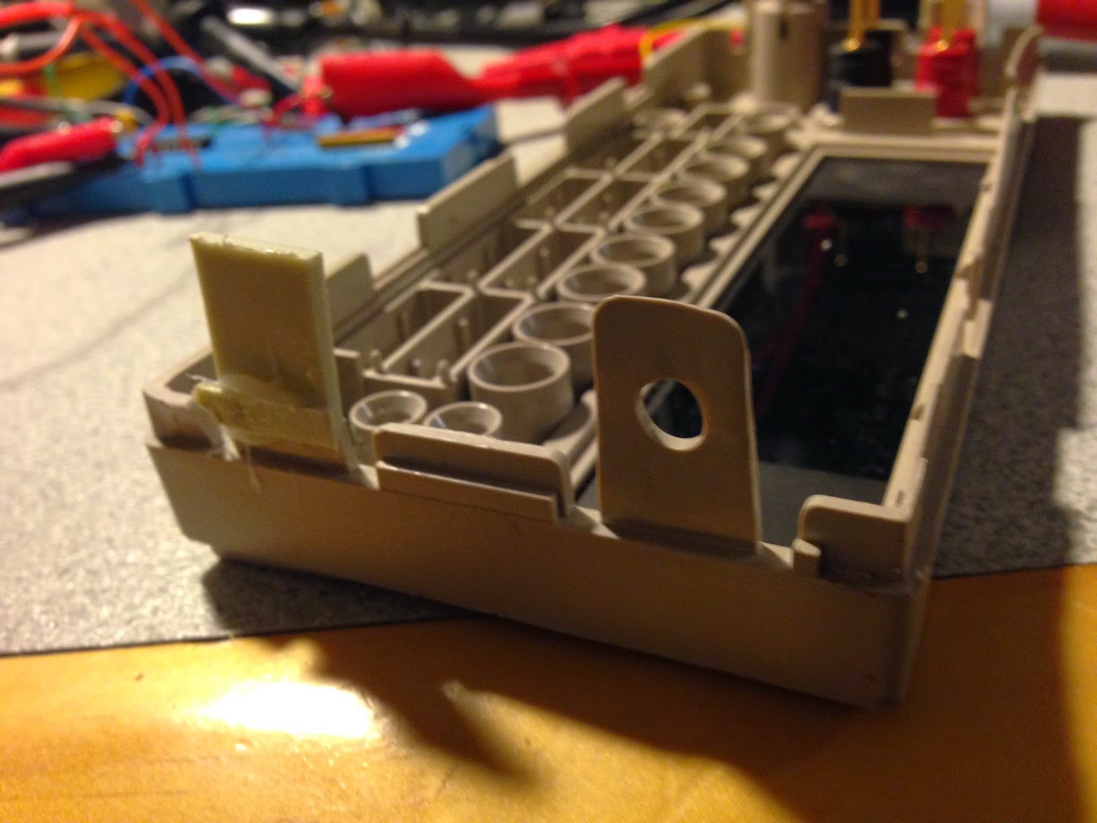
In my case when the unit was hit the front panel was ripped off and the tabs broke off. One tab was still intact but was bent out of shape.  A bit of heat from my surface mount solder blower sorted it out.


I thought if I could glue on some replacement tabs this might hold. After all they are just there to hold the front panel on. I asked on EEVBlog Forum about the best plastic to use and frankly I was overwhelmed with the response! One guy offered to give me a front panel from another model!

Another guy suggested a product called Devcon Plastic Welder. This isn't a normal hardware store item here in Australia so I had to order it but it was here in a few days.

I found an old drive bay cover from a PC case that had a similar feeling plastic. The plastic was the right thickness too at around 2mm.
I used a hacksaw to cut tabs out of this material that were 15mm wide. I cut off the broken tabs so they were flush with the adjacent plastic. My thinking was that they are thicker at the bottom and I would get a better glue bond with the thicker cross section.


I use the plastic welder to glue on the tabs I cut and I glued some small off-cuts to the outside for support.


 I let this all dry overnight and carefully measure the unbroken tab and the pins they lock onto. The pin diameter I measure to be 6.5mm but in the end I used 7mm to get a good fit. The tabs are 15mm wide and 30mm apart, The holes are dead centre and 28mm up from the ledge in the plastic.

The front foot support bolts over the top of these so you won't seem them when they are done. Unfortunately there wasn't enough clearance to leave the support material in place so I carefully dremeled it off.

I measured and marked up the hole locations, drilled a 1mm pilot hole as accurately as I could and then drilled the 7mm hole.  I test fitted a couple of times and had to ream a fraction here and there. I did mark the current probe tower with the drill bit but didn't cut through it.

After some monkeying around the front panel went on quite well and holds quite firmly.

I'd call that a success!

I carefully re-attached all the wires, straightened out the bent power push rod with a little heat and re-assembled it all. It's tricky to pass get the switch rods, wires and everything all back in at once but with a little patience it all snaps together. I put the lid back on and the back cover.

I powered it on and ran through some tests and it works! And looks Ok!


More Photos

Before I put it all back together I snapped a few more photos of the board. I haven't had much of a chance to really look at it much but it seems pretty nicely made. Some fancy precision resistors plus a gas discharge tube in the background. Not sure about the big pile of high wattage surface mount resistors in the foreground. 


Precision voltage reference plus some bridge rectifiers that are likely part of the RMS converter.


Xilinx Spartan FPGA plus associated RAM. Is that a programming header? Main processor is just above and it is a Coldfire MCF5407 Is that a programming header?

Net+ARM handles the Ethernet interface. Note the routing between the digital and analog parts of the board.


Part of the board is under that Aluminium shield. Note the big resistors with their own bit of exposed copper for (presumably) heat sinking.


Lots of PSU circuit on the digital side. Only a small amount on the analog side. The front end analog switching relays are *really* loud.


The End

So now I am left waiting for the benchkit so I can replace the broken front foot. At that point it is ready to go.

I really should sell it. No really. Ok maybe I can play with it while I am waiting for the bench kit.